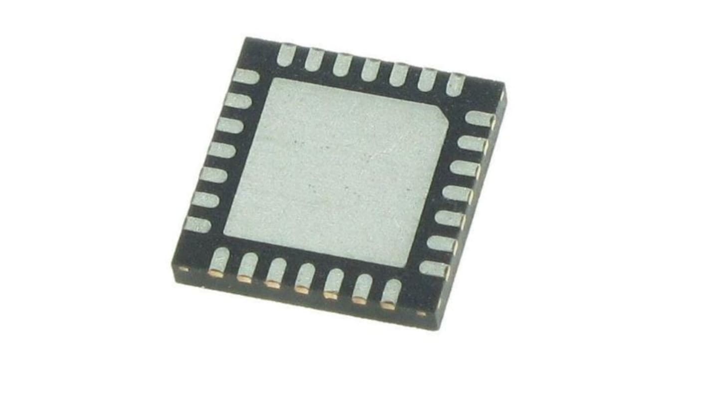
Renesas Electronics 8SLVP1208ANBGI Clock Buffer, 28-Pin LFCSP
- RS-stocknr.:
- 216-6232
- Fabrikantnummer:
- 8SLVP1208ANBGI
- Fabrikant:
- Renesas Electronics

Subtotaal (1 tray van 490 eenheden)*
€ 2.331,42
(excl. BTW)
€ 2.820,93
(incl. BTW)
GRATIS bezorging voor bestellingen van meer dan € 90,00
Tijdelijk niet op voorraad
- Verzending vanaf 12 maart 2027
Heeft u meer nodig? Klik op 'Controleer leverdata' voor extra voorraad en levertijden.
Aantal stuks | Per stuk | Per tray* |
|---|---|---|
| 490 + | € 4,758 | € 2.331,42 |
*prijsindicatie
- RS-stocknr.:
- 216-6232
- Fabrikantnummer:
- 8SLVP1208ANBGI
- Fabrikant:
- Renesas Electronics
Specificaties
Datasheets
Wetgeving en compliance
Productomschrijving
Zoek vergelijkbare producten door een of meer kenmerken te selecteren.
Alles selecteren | Attribuut | Waarde |
|---|---|---|
| Merk | Renesas Electronics | |
| Product Type | Clock Buffer | |
| Mount Type | Surface | |
| Package Type | LFCSP | |
| Pin Count | 28 | |
| Minimum Supply Voltage | 2.5V | |
| Maximum Supply Voltage | 3.3V | |
| Minimum Operating Temperature | -40°C | |
| Maximum Operating Temperature | 85°C | |
| Series | 8SLVP1208 | |
| Standards/Approvals | No | |
| Height | 0.7mm | |
| Length | 5mm | |
| Automotive Standard | No | |
| Alles selecteren | ||
|---|---|---|
Merk Renesas Electronics | ||
Product Type Clock Buffer | ||
Mount Type Surface | ||
Package Type LFCSP | ||
Pin Count 28 | ||
Minimum Supply Voltage 2.5V | ||
Maximum Supply Voltage 3.3V | ||
Minimum Operating Temperature -40°C | ||
Maximum Operating Temperature 85°C | ||
Series 8SLVP1208 | ||
Standards/Approvals No | ||
Height 0.7mm | ||
Length 5mm | ||
Automotive Standard No | ||
The Renesas Electronics 8SLVP1208 is a high-performance differential LVPECL fanout buffer. The device is designed for the fanout of high-frequency, very low additive phase-noise clock and data signals. The 8SLVP1208 is characterized to operate from a 3.3V and 2.5V power supply. Guaranteed output-to-output and part-to-part skew characteristics make the 8SLVP1208 ideal for those clock distribution applications demanding well-defined performance and repeatability.
Eight low skew, low additive jitter LVPECL output pairs
Two selectable, differential clock input pairs
Differential pairs can accept the following differential input
levels: LVDS, LVPECL, CML
Maximum input clock frequency: 2GHz
LVCMOS interface levels for the control input (input select)
Output skew: 28ps (typical)
Propagation delay: 410ps (maximum)
Low additive phase jitter, RMS: 54.1fs (maximum)
(fREF = 156.25MHz, VPP = 1V, 12kHz - 20MHz)
Gerelateerde Links
- Renesas Electronics 8SLVP1208ANBGI Clock Buffer, 28-Pin LFCSP
- Renesas Electronics Clock Buffer 28-Pin TSSOP
- Renesas Electronics Clock Buffer 28-Pin SSOP
- Renesas Electronics 9DB403DFILFT PLL Clock Buffer 28-Pin SSOP-28
- Renesas Electronics 9DB403DFLFT PLL Clock Buffer 28-Pin SSOP-28
- Renesas Electronics 9DB106BGILFT PLL Clock Buffer 28-Pin TSSOP-28
- Renesas Electronics 9DB403DGLFT Clock Buffer 28-Pin TSSOP
- Renesas Electronics 9DB433AGLF Clock Buffer 28-Pin TSSOP