onsemi MC14572UBDR2G, 6 2-Input Multifunction Logic Gate, 16-Pin SOIC
- RS-stocknr.:
- 163-0553
- Fabrikantnummer:
- MC14572UBDR2G
- Fabrikant:
- onsemi

Momenteel niet beschikbaar
We weten niet of dit artikel weer voorradig zal zijn, het wordt door de fabrikant stopgezet.
- RS-stocknr.:
- 163-0553
- Fabrikantnummer:
- MC14572UBDR2G
- Fabrikant:
- onsemi
Specificaties
Datasheets
Wetgeving en compliance
Productomschrijving
Zoek vergelijkbare producten door een of meer kenmerken te selecteren.
Alles selecteren | Attribuut | Waarde |
|---|---|---|
| Merk | onsemi | |
| Product Type | Logic Gate | |
| Logic Function | Multifunction | |
| Number of Elements | 6 | |
| Number of Inputs per Gate | 2 | |
| Schmitt Trigger Input | No | |
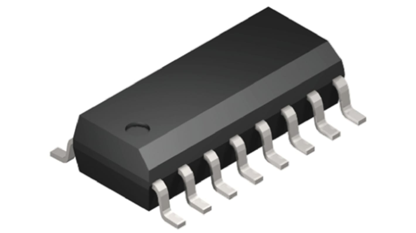
| Package Type | SOIC | |
| Pin Count | 16 | |
| Minimum Operating Temperature | -55°C | |
| Maximum High Level Output Current | -0.14mA | |
| Maximum Operating Temperature | 125°C | |
| Height | 1.5mm | |
| Length | 10mm | |
| Width | 4 mm | |
| Output Type | Single Ended | |
| Alles selecteren | ||
|---|---|---|
Merk onsemi | ||
Product Type Logic Gate | ||
Logic Function Multifunction | ||
Number of Elements 6 | ||
Number of Inputs per Gate 2 | ||
Schmitt Trigger Input No | ||
Package Type SOIC | ||
Pin Count 16 | ||
Minimum Operating Temperature -55°C | ||
Maximum High Level Output Current -0.14mA | ||
Maximum Operating Temperature 125°C | ||
Height 1.5mm | ||
Length 10mm | ||
Width 4 mm | ||
Output Type Single Ended | ||
- Land van herkomst:
- PH
The MC14572UB hex functional gate is constructed with MOS P-channel and N-channel enhancement mode devices in a single monolithic structure. These complementary MOS logic gates find primary use where low power dissipation and/or high noise immunity is desired. The chip contains four inverters, one NOR gate and one NAND gate.
Diode Protection on All Inputs
Single Supply Operation
Supply Voltage Range = 3.0 Vdc to 18 Vdc
NOR Input Pin Adjacent to VSS Pin to Simplify Use As An Inverter
NAND Input Pin Adjacent to VDD Pin to Simplify Use As An Inverter
NOR Output Pin Adjacent to Inverter Input Pin For OR Application
NAND Output Pin Adjacent to Inverter Input Pin For AND Application
Capable of Driving Two Low-power TTL Loads or One Low-Power Schottky TTL Load over the Rated Temperature Range