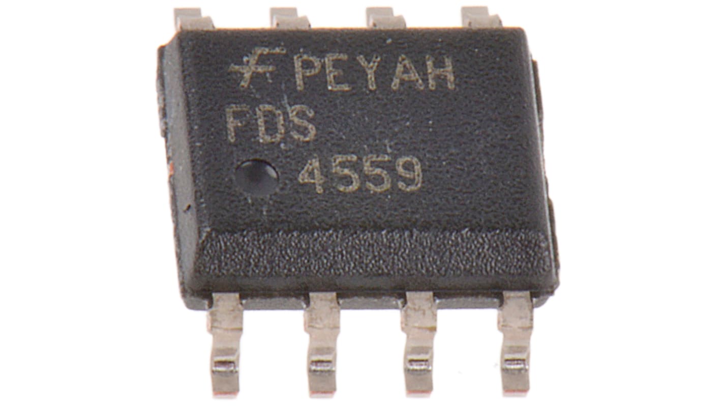
onsemi PowerTrench Dual N/P-Channel MOSFET, 3.5 A, 4.5 A, 60 V, 8-Pin SOIC FDS4559-F085
- RS-stocknr.:
- 864-8647
- Fabrikantnummer:
- FDS4559-F085
- Fabrikant:
- onsemi

Informatie over voorraden is momenteel niet toegankelijk
- RS-stocknr.:
- 864-8647
- Fabrikantnummer:
- FDS4559-F085
- Fabrikant:
- onsemi
Specificaties
Datasheets
Wetgeving en compliance
Zoek vergelijkbare producten door een of meer kenmerken te selecteren.
Alles selecteren | Attribuut | Waarde |
|---|---|---|
| Merk | onsemi | |
| Channel Type | N, P | |
| Maximum Continuous Drain Current | 3.5 A, 4.5 A | |
| Maximum Drain Source Voltage | 60 V | |
| Package Type | SOIC | |
| Series | PowerTrench | |
| Mounting Type | Surface Mount | |
| Pin Count | 8 | |
| Maximum Drain Source Resistance | 94 mΩ, 190 mΩ | |
| Channel Mode | Enhancement | |
| Minimum Gate Threshold Voltage | 1V | |
| Maximum Power Dissipation | 2 W | |
| Transistor Configuration | Isolated | |
| Maximum Gate Source Voltage | -20 V, +20 V | |
| Width | 3.9mm | |
| Typical Gate Charge @ Vgs | 12.5 nC @ 10 V, 15 nC @ 10 V | |
| Transistor Material | Si | |
| Number of Elements per Chip | 2 | |
| Length | 4.9mm | |
| Maximum Operating Temperature | +150 °C | |
| Minimum Operating Temperature | -55 °C | |
| Height | 1.575mm | |
| Alles selecteren | ||
|---|---|---|
Merk onsemi | ||
Channel Type N, P | ||
Maximum Continuous Drain Current 3.5 A, 4.5 A | ||
Maximum Drain Source Voltage 60 V | ||
Package Type SOIC | ||
Series PowerTrench | ||
Mounting Type Surface Mount | ||
Pin Count 8 | ||
Maximum Drain Source Resistance 94 mΩ, 190 mΩ | ||
Channel Mode Enhancement | ||
Minimum Gate Threshold Voltage 1V | ||
Maximum Power Dissipation 2 W | ||
Transistor Configuration Isolated | ||
Maximum Gate Source Voltage -20 V, +20 V | ||
Width 3.9mm | ||
Typical Gate Charge @ Vgs 12.5 nC @ 10 V, 15 nC @ 10 V | ||
Transistor Material Si | ||
Number of Elements per Chip 2 | ||
Length 4.9mm | ||
Maximum Operating Temperature +150 °C | ||
Minimum Operating Temperature -55 °C | ||
Height 1.575mm | ||
Gerelateerde Links
- onsemi Isolated PowerTrench 2 Type P 4.5 A 8-Pin SOIC FDS4559
- onsemi Isolated PowerTrench 2 Type P 4.5 A 8-Pin SOIC
- onsemi PowerTrench Dual N/P-Channel MOSFET 700 mA 6-Pin SOT-363 (SC-70) FDG6332C-F085
- onsemi PowerTrench P-Channel MOSFET 40 V, 8-Pin SOIC FDS4675-F085
- onsemi PowerTrench N-Channel MOSFET 40 V, 3-Pin DPAK FDD8444L-F085
- onsemi PowerTrench N-Channel MOSFET 150 V, 8-Pin PSOF FDBL86210-F085
- onsemi PowerTrench N-Channel MOSFET 100 V, 3-Pin DPAK FDD3682-F085
- onsemi PowerTrench Type P-Channel MOSFET 20 V Enhancement, 6-Pin SOT-23