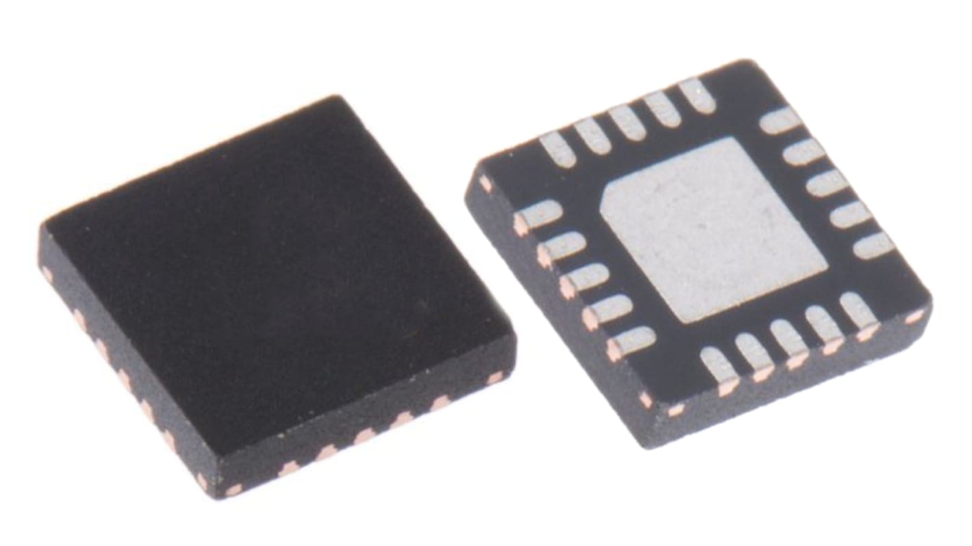
Renesas Electronics 5PB1216NDGK Clock Buffer 20-Pin VFQFPN
- RS-stocknr.:
- 262-8967P
- Fabrikantnummer:
- 5PB1216NDGK
- Fabrikant:
- Renesas Electronics

Bulkkorting beschikbaar
Subtotaal 10 eenheden (geleverd op een tray)*
€ 33,95
(excl. BTW)
€ 41,08
(incl. BTW)
GRATIS bezorging voor bestellingen van meer dan € 75,00
Tijdelijk niet op voorraad
- Verzending vanaf 16 juni 2026
Heeft u meer nodig? Klik op 'Controleer leverdata' voor extra voorraad en levertijden.
Aantal stuks | Per stuk |
|---|---|
| 10 - 48 | € 3,395 |
| 50 - 98 | € 3,235 |
| 100 - 248 | € 2,795 |
| 250 + | € 2,645 |
*prijsindicatie
- RS-stocknr.:
- 262-8967P
- Fabrikantnummer:
- 5PB1216NDGK
- Fabrikant:
- Renesas Electronics
Specificaties
Datasheets
Wetgeving en compliance
Productomschrijving
Zoek vergelijkbare producten door een of meer kenmerken te selecteren.
Alles selecteren | Attribuut | Waarde |
|---|---|---|
| Merk | Renesas Electronics | |
| Product Type | Clock Buffer | |
| Maximum Input Frequency | 200MHz | |
| Maximum Propagation Delay Time | 2.7ns | |
| Package Type | VFQFPN | |
| Pin Count | 20 | |
| Minimum Supply Voltage | 1.8V | |
| Maximum Supply Voltage | 3.8V | |
| Minimum Operating Temperature | -40°C | |
| Maximum Operating Temperature | 105°C | |
| Series | 5PB12xx | |
| Standards/Approvals | RoHS | |
| Width | 3 mm | |
| Length | 3mm | |
| Height | 1mm | |
| Automotive Standard | No | |
| Alles selecteren | ||
|---|---|---|
Merk Renesas Electronics | ||
Product Type Clock Buffer | ||
Maximum Input Frequency 200MHz | ||
Maximum Propagation Delay Time 2.7ns | ||
Package Type VFQFPN | ||
Pin Count 20 | ||
Minimum Supply Voltage 1.8V | ||
Maximum Supply Voltage 3.8V | ||
Minimum Operating Temperature -40°C | ||
Maximum Operating Temperature 105°C | ||
Series 5PB12xx | ||
Standards/Approvals RoHS | ||
Width 3 mm | ||
Length 3mm | ||
Height 1mm | ||
Automotive Standard No | ||
- Land van herkomst:
- TH
The Renesas Electronics Mix signal is a high-performance TCXO / LVCMOS clock fan-out buffer with individual OE pin for each output. The CLKIN pin can accept either a square wave or clipped sine wave as input. The mix signal has industry-leading low jitter and extremely low current consumption, making it ideal for smart mobile devices.
Extremely low operating and standby current consumption
Low RMS additive phase jitter
2.5 V to 3.3 V power supply voltage
Six outputs with individual output enable pin
OE_OSC control pin to enable/disable reference TCXO / XO
Small 20-pin VFQFPN package
Extended temperature range -40°C to +105°C
Gerelateerde Links
- Renesas Electronics 5PB1216NDGK Clock Buffer 20-Pin VFQFPN
- Renesas Electronics 9DBL0455NLGI Clock Buffer 20-Pin VFQFPN
- Renesas Electronics Clock Buffer 16-Pin VFQFPN
- Renesas Electronics 9FGV0641AKILF Clock Buffer 40-Pin VFQFPN
- Renesas Electronics 9DBV0231AKLF Clock Buffer 24-Pin VFQFPN
- Renesas Electronics 9DBL0951BKILF Clock Buffer 48-Pin VFQFPN
- Renesas Electronics 9DBV0831AKILF Clock Buffer 48-Pin VFQFPN
- Renesas Electronics 9ZXL0652EKILF Clock Buffer 40-Pin VFQFPN