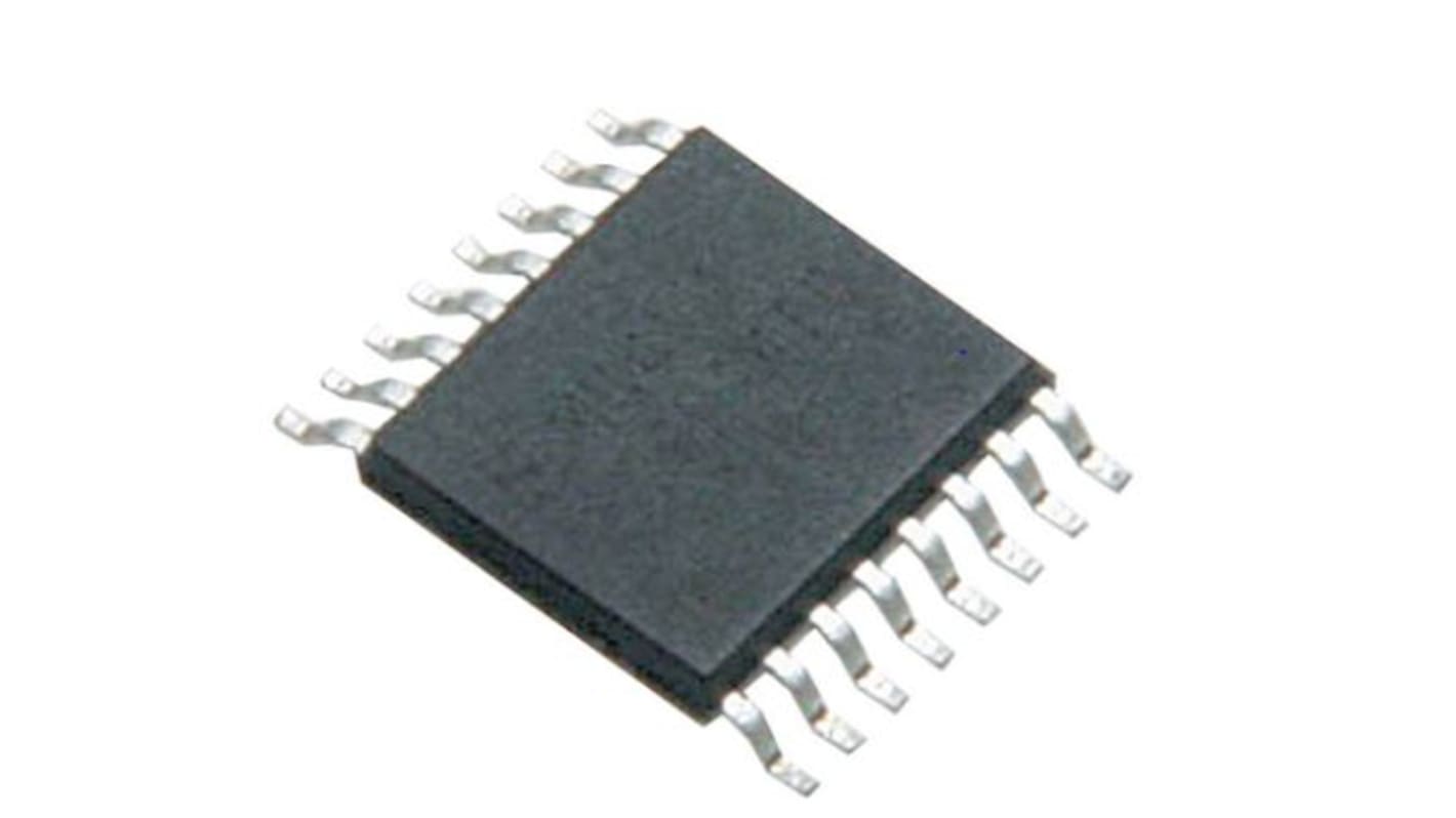
Renesas Electronics 5PB1108PGGI Clock Buffer, 16-Pin 8 VFQFPN
- RS-stocknr.:
- 216-6183
- Fabrikantnummer:
- 5PB1108PGGI
- Fabrikant:
- Renesas Electronics

Subtotaal (1 tube van 96 eenheden)*
€ 168,768
(excl. BTW)
€ 204,192
(incl. BTW)
GRATIS bezorging voor bestellingen van meer dan € 90,00
Laatste voorraad RS
- Laatste 96 stuk(s), klaar voor verzending vanaf een andere locatie
Aantal stuks | Per stuk | Per tube* |
|---|---|---|
| 96 + | € 1,758 | € 168,77 |
*prijsindicatie
- RS-stocknr.:
- 216-6183
- Fabrikantnummer:
- 5PB1108PGGI
- Fabrikant:
- Renesas Electronics
Specificaties
Datasheets
Wetgeving en compliance
Productomschrijving
Zoek vergelijkbare producten door een of meer kenmerken te selecteren.
Alles selecteren | Attribuut | Waarde |
|---|---|---|
| Merk | Renesas Electronics | |
| Product Type | Clock Buffer | |
| Mount Type | Surface | |
| Package Type | VFQFPN | |
| Minimum Supply Voltage | 1.8V | |
| Pin Count | 16 | |
| Maximum Supply Voltage | 3.3V | |
| Minimum Operating Temperature | -40°C | |
| Maximum Operating Temperature | 105°C | |
| Standards/Approvals | No | |
| Height | 1mm | |
| Length | 5mm | |
| Series | 5PB1108 | |
| Maximum Output Frequency | 200MHz | |
| Automotive Standard | No | |
| Alles selecteren | ||
|---|---|---|
Merk Renesas Electronics | ||
Product Type Clock Buffer | ||
Mount Type Surface | ||
Package Type VFQFPN | ||
Minimum Supply Voltage 1.8V | ||
Pin Count 16 | ||
Maximum Supply Voltage 3.3V | ||
Minimum Operating Temperature -40°C | ||
Maximum Operating Temperature 105°C | ||
Standards/Approvals No | ||
Height 1mm | ||
Length 5mm | ||
Series 5PB1108 | ||
Maximum Output Frequency 200MHz | ||
Automotive Standard No | ||
The Renesas Electronics 5PB11xx is a high-performance LVCMOS clock buffer family of devices. It has an additive phase jitter of 50fs RMS. There are five different fan-out variations available: 1:2 to 1:10. The 5PB11xx supports a synchronous glitch-free output enable (OE) function to eliminate any potential intermediate incorrect output clock cycles when enabling or disabling outputs. It can operate from a 1.8V to 3.3V supply.
High-performance 1:2, 1:4, 1:6, 1:8, 1:10 LVCMOS clock buffer
Very low pin-to-pin skew: < 50ps
Very low additive jitter: < 50fs
Supply voltage: 1.8V to 3.3V
3.3V tolerant input clock
fMAX = 200MHz
Integrated serial termination for 50Ω channel
Gerelateerde Links
- Renesas Electronics 5PB1108PGGI Clock Buffer, 16-Pin 8 VFQFPN
- Renesas Electronics 5PB1108CMGI Clock Buffer, 16-Pin 8 VFQFPN
- Renesas Electronics 9DMV0141AKILF Clock Buffer, 16-Pin 1 VFQFPN
- Renesas Electronics 5PB1106CMGI Clock Buffer, 16-Pin 4 VFQFPN
- Renesas Electronics Clock Buffer 16-Pin VFQFPN
- Renesas Electronics 5PB1204CMGK Clock Buffer 16-Pin VFQFPN
- Renesas Electronics 5PB1214CMGK Clock Buffer 16-Pin VFQFPN
- Renesas Electronics 5V2305PGGI Clock Buffer 16-Pin VFQFPN