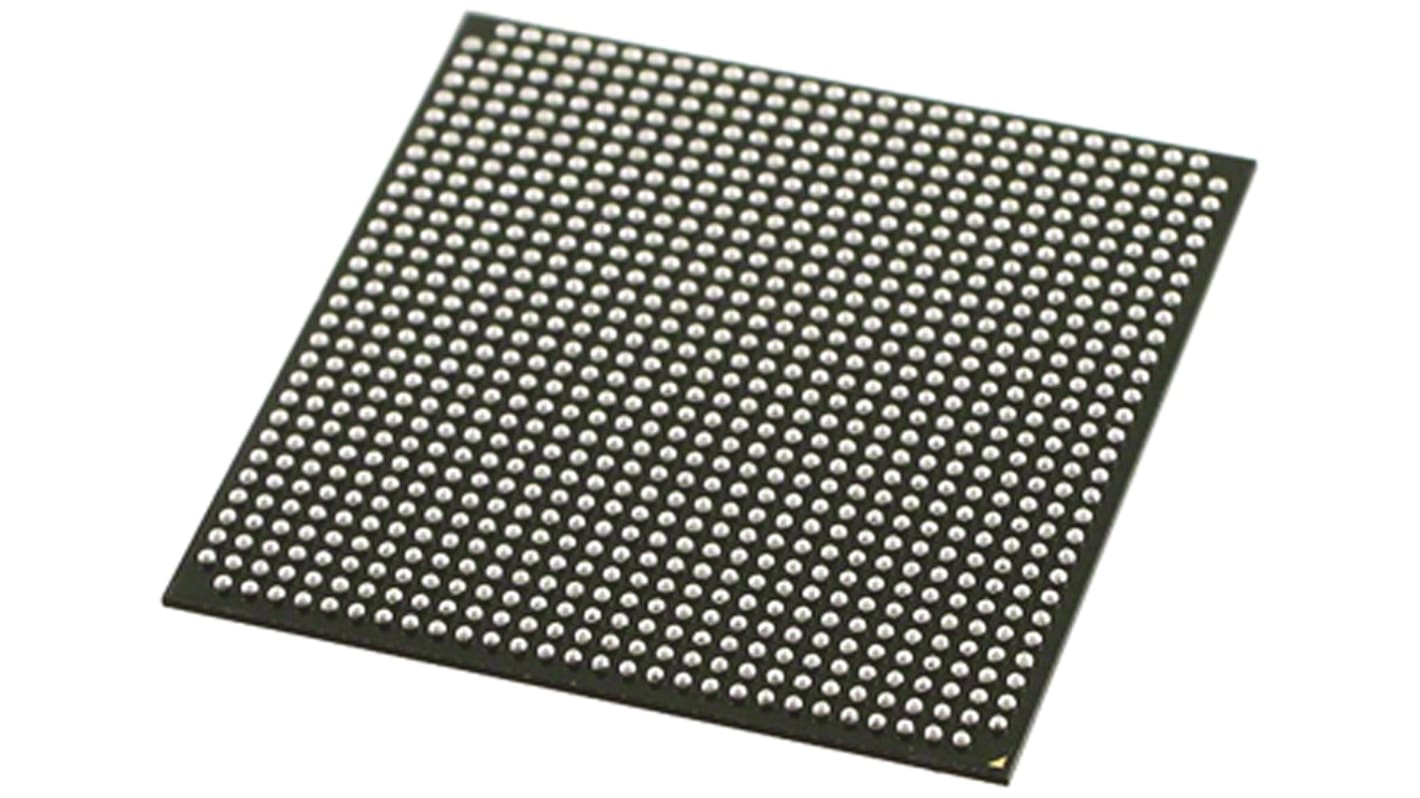
Altera FPGA 5CSEMA6F31C8N, Cyclone V SE 110000 Cells, 110000 Gates, 5761K, 41509 Blocks, 896-Pin FBGA
- RS-stocknr.:
- 830-3574
- Fabrikantnummer:
- 5CSEMA6F31C8N
- Fabrikant:
- Altera

Informatie over voorraden is momenteel niet toegankelijk
- RS-stocknr.:
- 830-3574
- Fabrikantnummer:
- 5CSEMA6F31C8N
- Fabrikant:
- Altera
Specificaties
Datasheets
Wetgeving en compliance
Zoek vergelijkbare producten door een of meer kenmerken te selecteren.
Alles selecteren | Attribuut | Waarde |
|---|---|---|
| Merk | Altera | |
| Family Name | Cyclone V SE | |
| Number of Logic Gates | 110000 | |
| Number of Logic Cells | 110000 | |
| Number of Logic Units | 41509 | |
| Dedicated DSP | Yes | |
| Number of Registers | 166036 | |
| Number of Multipliers | 224 (18 x 18) | |
| Mounting Type | Surface Mount | |
| Package Type | FBGA | |
| Pin Count | 896 | |
| Number of RAM Bits | 5761K | |
| Length | 31mm | |
| Maximum Operating Temperature | +85 °C | |
| Minimum Operating Temperature | 0 °C | |
| Maximum Operating Supply Voltage | 3.3 V | |
| Minimum Operating Supply Voltage | 1.8 V | |
| Width | 31mm | |
| Alles selecteren | ||
|---|---|---|
Merk Altera | ||
Family Name Cyclone V SE | ||
Number of Logic Gates 110000 | ||
Number of Logic Cells 110000 | ||
Number of Logic Units 41509 | ||
Dedicated DSP Yes | ||
Number of Registers 166036 | ||
Number of Multipliers 224 (18 x 18) | ||
Mounting Type Surface Mount | ||
Package Type FBGA | ||
Pin Count 896 | ||
Number of RAM Bits 5761K | ||
Length 31mm | ||
Maximum Operating Temperature +85 °C | ||
Minimum Operating Temperature 0 °C | ||
Maximum Operating Supply Voltage 3.3 V | ||
Minimum Operating Supply Voltage 1.8 V | ||
Width 31mm | ||
Gerelateerde Links
- Altera FPGA 5CSXFC5D6F31C8N 85000 Gates 32075 Blocks, 896-Pin FBGA
- Altera FPGA EP1C6F256I7N 5980 Blocks, 256-Pin FBGA
- Altera FPGA Cyclone III 15408 Cells 484-Pin FBGA
- Altera FPGA EP3C16F484C8N Cyclone III 15408 Cells 484-Pin FBGA
- Altera FPGA Cyclone IV 28848 Cells 484-Pin FBGA
- Altera FPGA Cyclone III 55856 Cells 484-Pin FBGA
- Altera FPGA EP4CE15F23I8LN 15408 Gates 963 Blocks, 484-Pin FBGA
- Altera FPGA EP4CE30F23C8N Cyclone IV 28848 Cells 484-Pin FBGA