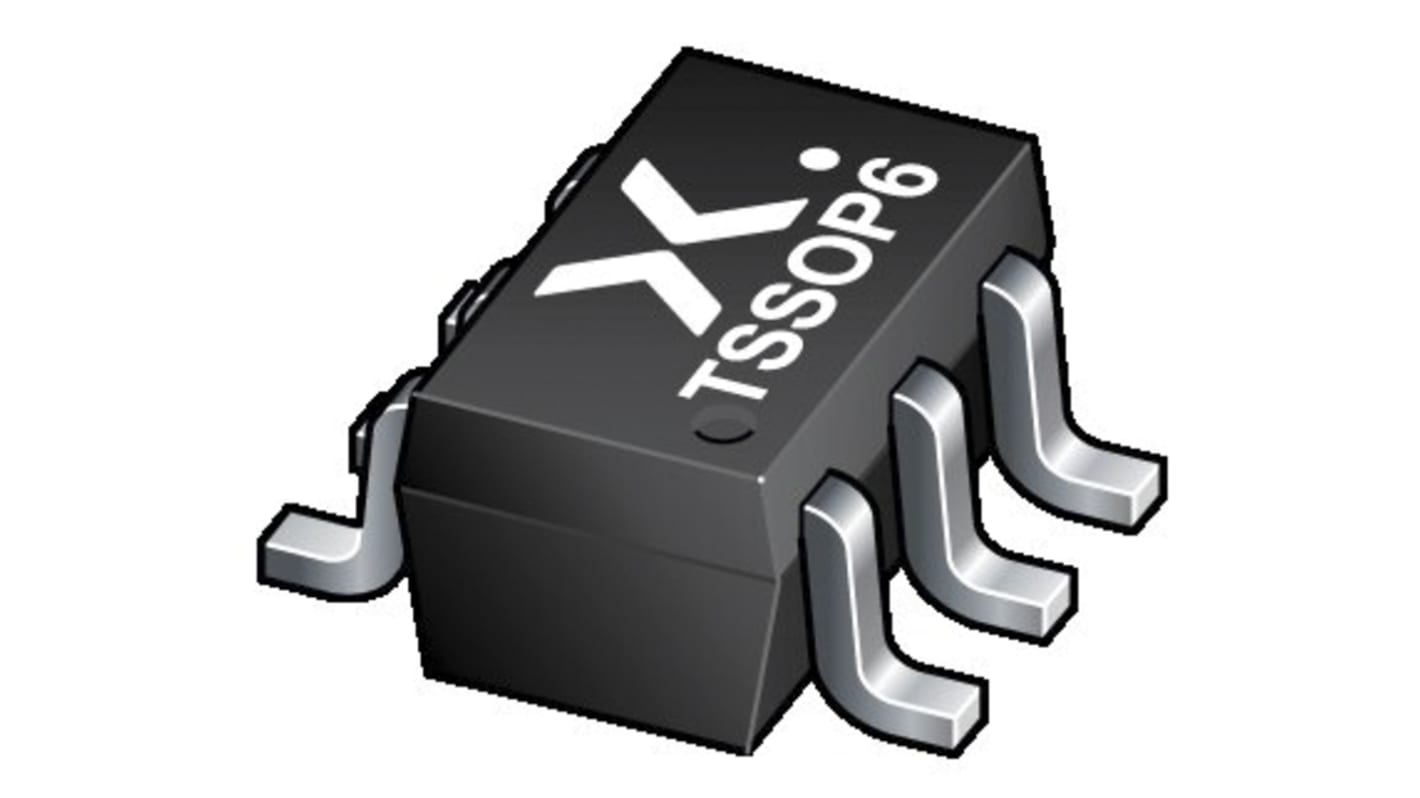
Nexperia 74LVC2G07GW,125 2-Channel Buffer & Line Driver, Open Drain, Non-Inverting, 6-Pin TSSOP
- RS-stocknr.:
- 182-1870
- Fabrikantnummer:
- 74LVC2G07GW,125
- Fabrikant:
- Nexperia

Bulkkorting beschikbaar
Bekijk bulkkortingSubtotaal (1 verpakking van 20 eenheden)*
€ 1,74
(excl. BTW)
€ 2,10
(incl. BTW)
GRATIS bezorging voor bestellingen van meer dan € 90,00
Tijdelijk niet op voorraad
- Verzending vanaf 01 september 2026
Heeft u meer nodig? Klik op 'Controleer leverdata' voor extra voorraad en levertijden.
Aantal stuks | Per stuk | Per verpakking* |
|---|---|---|
| 20 - 80 | € 0,087 | € 1,74 |
| 100 - 480 | € 0,084 | € 1,68 |
| 500 - 980 | € 0,082 | € 1,64 |
| 1000 - 1980 | € 0,08 | € 1,60 |
| 2000 + | € 0,078 | € 1,56 |
*prijsindicatie
- RS-stocknr.:
- 182-1870
- Fabrikantnummer:
- 74LVC2G07GW,125
- Fabrikant:
- Nexperia
Specificaties
Datasheets
Wetgeving en compliance
Productomschrijving
Zoek vergelijkbare producten door een of meer kenmerken te selecteren.
Alles selecteren | Attribuut | Waarde |
|---|---|---|
| Merk | Nexperia | |
| Product Type | Buffer & Line Driver | |
| Logic Family | 74LVC | |
| Logic Function | Buffer | |
| IC Type | Buffer & Line Driver IC | |
| Number of Channels | 2 | |
| Input Type | Schmitt Trigger | |
| Output Type | Open Drain | |
| Polarity | Non-Inverting | |
| Mount Type | Surface | |
| Package Type | TSSOP | |
| Pin Count | 6 | |
| Minimum Supply Voltage | 1.65V | |
| Maximum Supply Voltage | 5.5V | |
| Minimum Operating Temperature | -40°C | |
| Maximum Propagation Delay Time @ CL | 3.7ns | |
| Maximum Low Level Output Current | 32mA | |
| Maximum Operating Temperature | 125°C | |
| Height | 1.1mm | |
| Length | 2.2mm | |
| Series | 74LVC2G07 | |
| Standards/Approvals | No | |
| Supply Current | 4μA | |
| Automotive Standard | No | |
| Alles selecteren | ||
|---|---|---|
Merk Nexperia | ||
Product Type Buffer & Line Driver | ||
Logic Family 74LVC | ||
Logic Function Buffer | ||
IC Type Buffer & Line Driver IC | ||
Number of Channels 2 | ||
Input Type Schmitt Trigger | ||
Output Type Open Drain | ||
Polarity Non-Inverting | ||
Mount Type Surface | ||
Package Type TSSOP | ||
Pin Count 6 | ||
Minimum Supply Voltage 1.65V | ||
Maximum Supply Voltage 5.5V | ||
Minimum Operating Temperature -40°C | ||
Maximum Propagation Delay Time @ CL 3.7ns | ||
Maximum Low Level Output Current 32mA | ||
Maximum Operating Temperature 125°C | ||
Height 1.1mm | ||
Length 2.2mm | ||
Series 74LVC2G07 | ||
Standards/Approvals No | ||
Supply Current 4μA | ||
Automotive Standard No | ||
- Land van herkomst:
- MY
The 74LVC2G07 provides two non-inverting buffers. The output of this device is an open drain and can be connected to other open-drain outputs to implement active-LOW wired-OR or active-HIGH wired-AND functions. Inputs can be driven from either 3.3 V or 5 V devices. This feature allows the use of this device in a mixed 3.3 V and 5 V environment. Schmitt trigger action at all inputs makes the circuit tolerant for slower input rise and fall time. This device is fully specified for partial power-down applications using IOFF. The IOFF circuitry disables the output, preventing the damaging backflow current through the device when it is powered down.
Wide supply voltage range from 1.65 V to 5.5 V
5 V tolerant input/output for interfacing with 5 V logic
High noise immunity
CMOS low power consumption
Latch-up performance exceeds 250 mA
Direct interface with TTL levels
Inputs accept voltages up to 5 V
Multiple package options
Specified from -40 °C to +85 °C and -40 °C to +125 °C
Gerelateerde Links
- Nexperia 2-Channel Buffer & Line Driver Non-Inverting, 6-Pin TSSOP
- Nexperia Buffer & Line Driver Non-Inverting, 5-Pin TSSOP
- Nexperia 74LVC1G07GW Open Drain 5-Pin TSSOP
- Nexperia 6-Channel Buffer & Line Driver Non-Inverting, 14-Pin TSSOP
- Nexperia 74LVC07APW Open Drain 14-Pin TSSOP
- Nexperia 74LVC07APW Open Drain 14-Pin TSSOP
- DiodesZetex Buffer & Line Driver Inverting, 5-Pin TSSOP
- DiodesZetex Buffer & Line Driver Non-Inverting, 5-Pin TSSOP