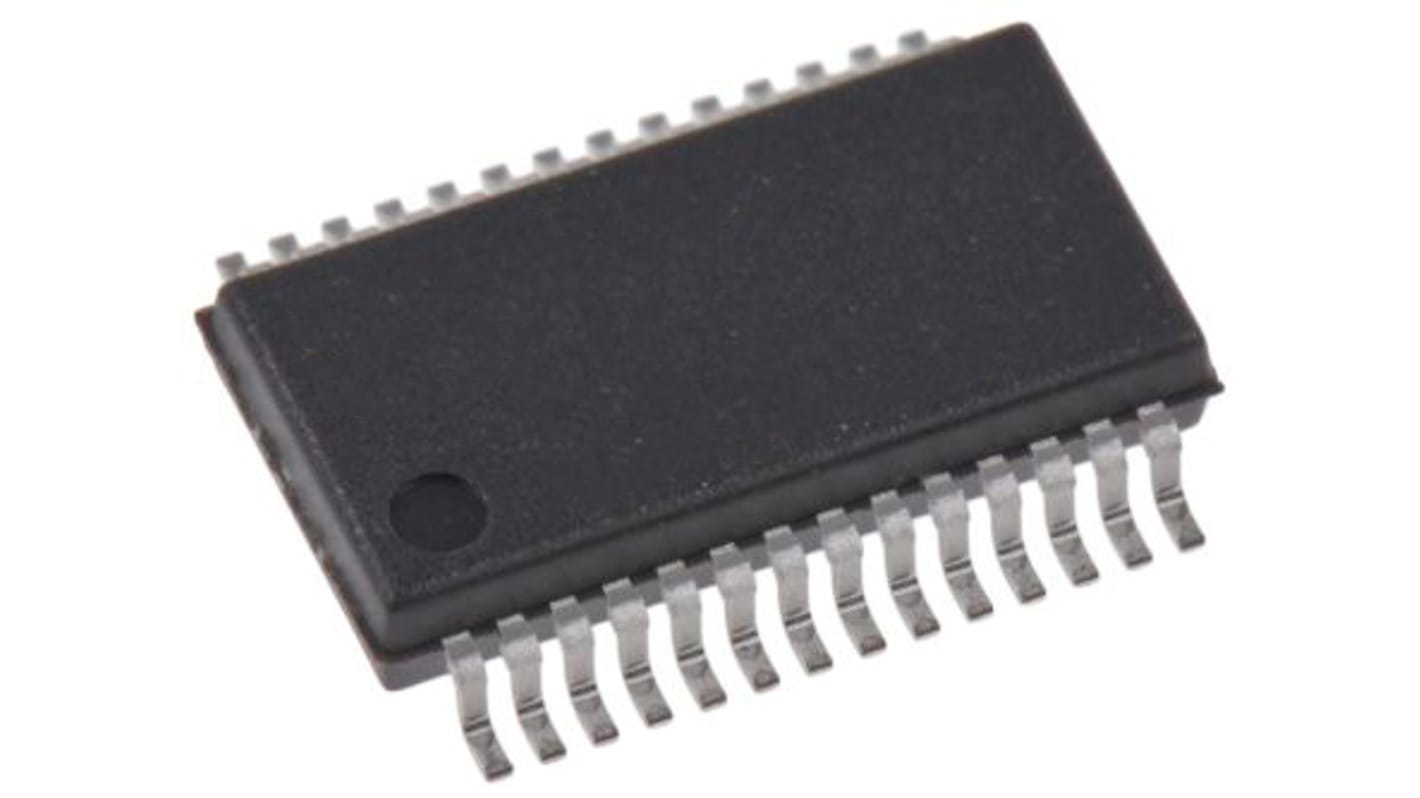
Infineon, 32bit ARM Cortex M0, CY8C4200 Microcontroller, 48MHz, 32 kB Flash, 28-Pin SSOP
- RS-stocknr.:
- 176-8968
- Fabrikantnummer:
- CY8C4045PVI-DS402
- Fabrikant:
- Infineon

Informatie over voorraden is momenteel niet toegankelijk
- RS-stocknr.:
- 176-8968
- Fabrikantnummer:
- CY8C4045PVI-DS402
- Fabrikant:
- Infineon
Specificaties
Datasheets
Wetgeving en compliance
Productomschrijving
Zoek vergelijkbare producten door een of meer kenmerken te selecteren.
Alles selecteren | Attribuut | Waarde |
|---|---|---|
| Merk | Infineon | |
| Family Name | CY8C4200 | |
| Package Type | SSOP | |
| Mounting Type | Surface Mount | |
| Pin Count | 28 | |
| Device Core | ARM Cortex M0 | |
| Data Bus Width | 32bit | |
| Program Memory Size | 32 kB | |
| Maximum Frequency | 48MHz | |
| RAM Size | 4 kB | |
| USB Channels | 0 | |
| Number of PWM Units | 1 x 16 bit | |
| Number of SPI Channels | 3 | |
| Typical Operating Supply Voltage | 1.8 → 5.5 V | |
| Number of UART Channels | 4 | |
| Number of I2C Channels | 4 | |
| Number of USART Channels | 0 | |
| Number of CAN Channels | 0 | |
| Number of ADC Units | 0 | |
| Maximum Operating Temperature | +85 °C | |
| Minimum Operating Temperature | -40 °C | |
| Instruction Set Architecture | Thumb-2 | |
| Maximum Number of Ethernet Channels | 0 | |
| Length | 10.4mm | |
| Width | 5.6mm | |
| Number of PCI Channels | 0 | |
| Height | 1.85mm | |
| Program Memory Type | Flash | |
| Number of Ethernet Channels | 0 | |
| Pulse Width Modulation | 1 (4 x 16 bit) | |
| Dimensions | 10.4 x 5.6 x 1.85mm | |
| Number of LIN Channels | 0 | |
| Alles selecteren | ||
|---|---|---|
Merk Infineon | ||
Family Name CY8C4200 | ||
Package Type SSOP | ||
Mounting Type Surface Mount | ||
Pin Count 28 | ||
Device Core ARM Cortex M0 | ||
Data Bus Width 32bit | ||
Program Memory Size 32 kB | ||
Maximum Frequency 48MHz | ||
RAM Size 4 kB | ||
USB Channels 0 | ||
Number of PWM Units 1 x 16 bit | ||
Number of SPI Channels 3 | ||
Typical Operating Supply Voltage 1.8 → 5.5 V | ||
Number of UART Channels 4 | ||
Number of I2C Channels 4 | ||
Number of USART Channels 0 | ||
Number of CAN Channels 0 | ||
Number of ADC Units 0 | ||
Maximum Operating Temperature +85 °C | ||
Minimum Operating Temperature -40 °C | ||
Instruction Set Architecture Thumb-2 | ||
Maximum Number of Ethernet Channels 0 | ||
Length 10.4mm | ||
Width 5.6mm | ||
Number of PCI Channels 0 | ||
Height 1.85mm | ||
Program Memory Type Flash | ||
Number of Ethernet Channels 0 | ||
Pulse Width Modulation 1 (4 x 16 bit) | ||
Dimensions 10.4 x 5.6 x 1.85mm | ||
Number of LIN Channels 0 | ||
PSoC® 4 is a scalable and reconfigurable platform architecture for a family of programmable embedded system controllers with an Arm® Cortex®-M0 CPU. It combines programmable and reconfigurable analog and digital blocks with flexible automatic routing. The PSoC 4200_BL product family, based on this platform, is a combination of a microcontroller with an integrated Bluetooth Low Energy (BLE), also known as Bluetooth Smart, radio and subsystem (BLESS).
Four opamps with reconfigurable high-drive external and high-bandwidth internal drive, Comparator modes, and ADC input buffering capability Can operate in Deep Sleep mode.
Four programmable logic blocks called universal digital blocks, (UDBs), each with eight macrocells and data path
Cypress-provided peripheral component library, user-defined state machines, and Verilog input
Power Management:
Active mode: 1.7 mA at 3-MHz flash program execution
Deep Sleep mode: 1.5 μA with watch crystal oscillator
Gerelateerde Links
- Infineon CY8C4200 Microcontroller 32 kB Flash, 28-Pin SSOP
- Infineon PSoC4100 Microcontroller 32 kB Flash, 28-Pin SSOP
- STMicroelectronics ARM Cortex M0+ Microcontroller 32 KB Flash, 48-Pin LQFP-48
- NXP Kinetis W Microcontroller 128 kB Flash, 60-Pin LGA
- NXP Kinetis L Microcontroller 32 kB Flash, 32-Pin QFN
- Texas Instruments SimpleLink Microcontroller 128 kB Flash, 48-Pin VQFN
- Renesas Electronics S3A3 Microcontroller 512 kB Flash, 64-Pin LQFP
- Silicon Labs EZR32WG Microcontroller 256 kB Flash, 64-Pin QFN