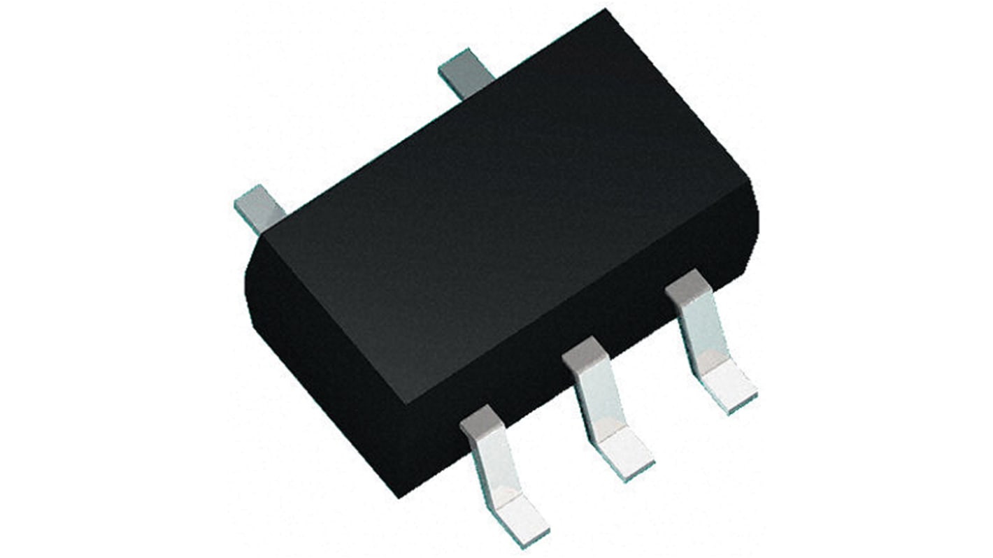
onsemi NLVSV1T34DFT2G, Logic Level Translator Voltage Level Translator, 5-Pin SC-88A
- RS-stocknr.:
- 172-3400P
- Fabrikantnummer:
- NLVSV1T34DFT2G
- Fabrikant:
- onsemi

Momenteel niet beschikbaar
We weten niet of dit item nog op voorraad komt, RS is van plan dit binnenkort uit ons assortiment te halen.
- RS-stocknr.:
- 172-3400P
- Fabrikantnummer:
- NLVSV1T34DFT2G
- Fabrikant:
- onsemi
Specificaties
Datasheets
Wetgeving en compliance
Productomschrijving
Zoek vergelijkbare producten door een of meer kenmerken te selecteren.
Alles selecteren | Attribuut | Waarde |
|---|---|---|
| Merk | onsemi | |
| Product Type | Logic Level Translator | |
| Logic Family | NLSV | |
| Mount Type | Surface | |
| Package Type | SC-88A | |
| Pin Count | 5 | |
| Output Type | Single Ended | |
| Logic Function | Voltage Level Translator | |
| Maximum Low Level Output Current | 24mA | |
| Maximum High Level Output Current | -24mA | |
| Minimum Operating Temperature | -40°C | |
| Maximum Operating Temperature | 85°C | |
| Length | 2.2mm | |
| Height | 1mm | |
| Width | 1.35mm | |
| Automotive Standard | AEC-Q100 | |
| Alles selecteren | ||
|---|---|---|
Merk onsemi | ||
Product Type Logic Level Translator | ||
Logic Family NLSV | ||
Mount Type Surface | ||
Package Type SC-88A | ||
Pin Count 5 | ||
Output Type Single Ended | ||
Logic Function Voltage Level Translator | ||
Maximum Low Level Output Current 24mA | ||
Maximum High Level Output Current -24mA | ||
Minimum Operating Temperature -40°C | ||
Maximum Operating Temperature 85°C | ||
Length 2.2mm | ||
Height 1mm | ||
Width 1.35mm | ||
Automotive Standard AEC-Q100 | ||
The NLSV1T34 is a 1-bit configurable dual supply voltage level translator. The input An and output Bn ports are designed to track two different power supply rails, VCCA and VCCB respectively. Both supply rails are configurable from 0.9 V to 4.5 V allowing universal low voltage translation from the input An to the output Bn port.
Wide VCCA and VCCB Operating Range: 0.9 V to 4.5 V
High-Speed w/ Balanced Propagation Delay
Inputs and Outputs have OVT Protection to 4.5 V
Non-preferential VCCA and VCCB Sequencing
Power-Off Protection
UltraSmall Packaging: 1.45 mm x 1.0 mm ULLGA6 2.0 mm x 2.1 mm SC88A 1.2 mm x 1.0 mm UDFN6 1.45 mm x 1.0 mm UDFN6
This is a Pb and Halide Free Device
Applications
Mobile Phones, PDAs, Other Portable Devices
Gerelateerde Links
- onsemi NLVSV1T34DFT2G 5-Pin SC-88A
- onsemi 5-Pin SC-88A
- onsemi NLSV1T34DFT2G 5-Pin SC-88A
- Nexperia 6-Pin SC-88
- onsemi NLSX4373DR2G 8-Pin SOIC
- onsemi NLSX4373DR2G 8-Pin SOIC
- Nexperia 74AVC1T45GW Logic Level Translator Voltage Level Translator 6 Voltage Level Translator/Transceiver, 6-Pin
- Maxim Integrated 6-Pin SCT0