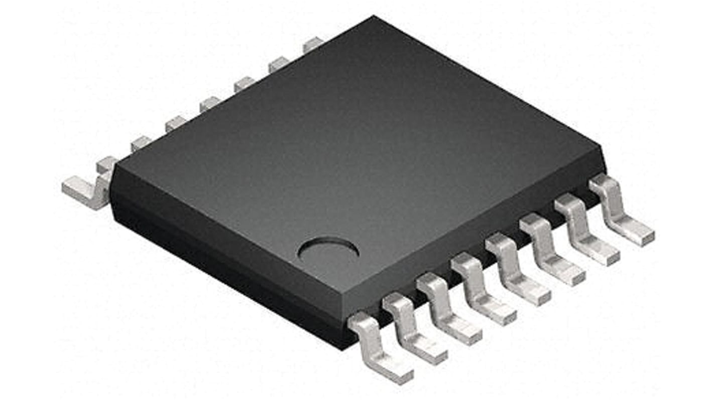
Toshiba 74VHC139FT, CMOS Digital Integrated Circuit 4 μA, 16-Pin TSSOP
- RS-stocknr.:
- 171-3447
- Fabrikantnummer:
- 74VHC139FT
- Fabrikant:
- Toshiba

Momenteel niet beschikbaar
We weten niet of dit item nog op voorraad komt, RS is van plan dit binnenkort uit ons assortiment te halen.
- RS-stocknr.:
- 171-3447
- Fabrikantnummer:
- 74VHC139FT
- Fabrikant:
- Toshiba
Specificaties
Datasheets
Wetgeving en compliance
Productomschrijving
Zoek vergelijkbare producten door een of meer kenmerken te selecteren.
Alles selecteren | Attribuut | Waarde |
|---|---|---|
| Merk | Toshiba | |
| Product Type | CMOS Digital Integrated Circuit | |
| Logic Family | 74VHC | |
| Logic Function | Decoder | |
| Number of Inputs | 3 | |
| Typical Supply Current | 4μA | |
| Mount Type | Surface | |
| Package Type | TSSOP | |
| Pin Count | 16 | |
| Minimum Supply Voltage | 2V | |
| Maximum Supply Voltage | 5.5V | |
| Minimum Operating Temperature | -40°C | |
| Maximum Operating Temperature | 125°C | |
| Series | 74VHC | |
| Length | 5mm | |
| Height | 1.2mm | |
| Standards/Approvals | AEC-Q100 | |
| Automotive Standard | AEC-Q100 | |
| Alles selecteren | ||
|---|---|---|
Merk Toshiba | ||
Product Type CMOS Digital Integrated Circuit | ||
Logic Family 74VHC | ||
Logic Function Decoder | ||
Number of Inputs 3 | ||
Typical Supply Current 4μA | ||
Mount Type Surface | ||
Package Type TSSOP | ||
Pin Count 16 | ||
Minimum Supply Voltage 2V | ||
Maximum Supply Voltage 5.5V | ||
Minimum Operating Temperature -40°C | ||
Maximum Operating Temperature 125°C | ||
Series 74VHC | ||
Length 5mm | ||
Height 1.2mm | ||
Standards/Approvals AEC-Q100 | ||
Automotive Standard AEC-Q100 | ||
The 74VHC139FT is an advanced high speed CMOS 2 to 4 LINE DECODER/DEMULTIPLEXER fabricated with silicon gate C2MOS technology. It achieves the high speed operation similar to equivalent Bipolar Schottky TTL while maintaining the CMOS low power dissipation. The active low enable input can be used for gating or it can be used as a data input for demultiplexing applications. When the enable input is held High, all four outputs are fixed at a high logic level independent of the other inputs. An input protection circuit ensures that 0 to 5.5 V can be applied to the input pins without regard to the supply voltage. This device can be used to interface 5 V to 3 V systems and two supply systems such as battery back up. This circuit prevents device destruction due to mismatched supply and input voltages.
Wide operating temperature: Topr = -40 to 125
High speed: Propagation delay time = 3.8 ns (typ.) at VCC = 5.0 V
Low power dissipation: ICC = 2.0 μA (max) at Ta = 25
High noise immunity: VNIH = VNIL = 28 % VCC (min)
Power-down protection is provided on all inputs.
Balanced propagation delays: tPLH ≈ tPHL
Wide operating voltage range: VCC(opr) = 2.0 to 5.5 V
Gerelateerde Links
- Toshiba 74VHC139FT 16-Pin TSSOP
- Toshiba 74LCX74FT 2 CMOS Digital Integrated Circuit 74LCX 14-Pin TSSOP
- Toshiba 74VHC05FT 6 CMOS Digital Integrated Circuit, 14-Pin TSSOP
- Toshiba 74VHCT14AFT 6 Schmitt Trigger Input CMOS Digital Integrated Circuit, 14-Pin TSSOP
- Toshiba 14-Pin TSSOP
- Toshiba 74VHCT32AFT 14-Pin TSSOP
- Toshiba 74VHC20FT 14-Pin TSSOP
- Toshiba 6 CMOS Digital Integrated Circuit, 14-Pin SOIC