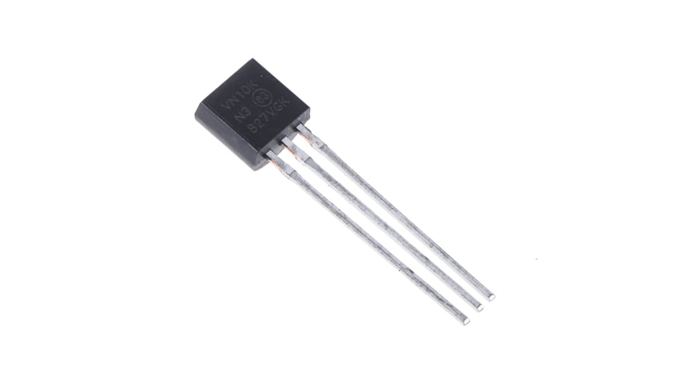
Microchip VN10K Type N-Channel MOSFET, 310 mA, 60 V Enhancement, 3-Pin TO-92 VN10KN3-G
- RS-stocknr.:
- 177-9716
- Artikelnummer Distrelec:
- 304-38-572
- Fabrikantnummer:
- VN10KN3-G
- Fabrikant:
- Microchip

Bulkkorting beschikbaar
Bekijk bulkkortingSubtotaal (1 verpakking van 25 eenheden)*
€ 13,50
(excl. BTW)
€ 16,25
(incl. BTW)
GRATIS bezorging voor bestellingen van meer dan € 90,00
Op voorraad
- 225 stuk(s) klaar voor verzending vanaf een andere locatie
- Plus verzending 175 stuk(s) vanaf 21 juli 2026
Heeft u meer nodig? Klik op 'Controleer leverdata' voor extra voorraad en levertijden.
Aantal stuks | Per stuk | Per verpakking* |
|---|---|---|
| 25 - 75 | € 0,54 | € 13,50 |
| 100 + | € 0,502 | € 12,55 |
*prijsindicatie
- RS-stocknr.:
- 177-9716
- Artikelnummer Distrelec:
- 304-38-572
- Fabrikantnummer:
- VN10KN3-G
- Fabrikant:
- Microchip
Specificaties
Datasheets
Wetgeving en compliance
Productomschrijving
Zoek vergelijkbare producten door een of meer kenmerken te selecteren.
Alles selecteren | Attribuut | Waarde |
|---|---|---|
| Merk | Microchip | |
| Channel Type | Type N | |
| Product Type | MOSFET | |
| Maximum Continuous Drain Current Id | 310mA | |
| Maximum Drain Source Voltage Vds | 60V | |
| Series | VN10K | |
| Package Type | TO-92 | |
| Mount Type | Through Hole | |
| Pin Count | 3 | |
| Maximum Drain Source Resistance Rds | 7.5Ω | |
| Channel Mode | Enhancement | |
| Forward Voltage Vf | 0.8V | |
| Minimum Operating Temperature | -55°C | |
| Maximum Power Dissipation Pd | 1W | |
| Maximum Operating Temperature | 150°C | |
| Length | 5.08mm | |
| Standards/Approvals | No | |
| Height | 5.33mm | |
| Automotive Standard | No | |
| Alles selecteren | ||
|---|---|---|
Merk Microchip | ||
Channel Type Type N | ||
Product Type MOSFET | ||
Maximum Continuous Drain Current Id 310mA | ||
Maximum Drain Source Voltage Vds 60V | ||
Series VN10K | ||
Package Type TO-92 | ||
Mount Type Through Hole | ||
Pin Count 3 | ||
Maximum Drain Source Resistance Rds 7.5Ω | ||
Channel Mode Enhancement | ||
Forward Voltage Vf 0.8V | ||
Minimum Operating Temperature -55°C | ||
Maximum Power Dissipation Pd 1W | ||
Maximum Operating Temperature 150°C | ||
Length 5.08mm | ||
Standards/Approvals No | ||
Height 5.33mm | ||
Automotive Standard No | ||
Microchip Technology MOSFET
The Microchip Technology through-hole mount N-channel MOSFET is a new age product with a drain-source resistance of 5ohms at a gate-source voltage of 10V. It has a drain-source voltage of 60V and a maximum gate-source voltage of 30V. It has continuous drain current of 310mA and maximum power dissipation of 1W. The minimum and a maximum driving voltage for this transistor are 5V and 10V respectively. The MOSFET is an enhancement mode (normally off) transistor that utilizes a vertical DMOS structure and well-proven, silicon gate manufacturing process. This combination produces a device with the power handling capabilities of bipolar transistors and the high input impedance and positive temperature coefficient inherent in MOS devices. A significant characteristic of all MOS structures, this device is free from thermal runaway and thermally induced secondary breakdown. This vertical DMOS FET has been optimized for lower switching and conduction losses. The MOSFET offers excellent efficiency along with a long and productive life without compromising performance or functionality.
Features and Benefits
• Ease of paralleling
• Excellent thermal stability
• Free from secondary breakdown
• High input impedance and high gain
• Integral source drain diode
• Low CISS and fast switching speeds
• Low power drive requirement
• Operating temperature ranges between -55°C and 150°C
Applications
• Amplifiers
• Converters
• Drivers (relays, hammers, solenoids, lamps, memories, displays, bipolar transistors, etc.)
• Motor controls
• Power supply circuits
• Switches
Certifications
• ANSI/ESD S20.20:2014
• BS EN 61340-5-1:2007
• JEDEC
Gerelateerde Links
- Microchip VN10K Type N-Channel MOSFET 60 V Enhancement, 3-Pin TO-92
- Microchip Type N-Channel MOSFET 60 V Enhancement, 3-Pin TO-92 VN2222LL-G
- Microchip 2N7008 Type N-Channel MOSFET 60 V Enhancement, 3-Pin TO-92 2N7008-G
- Microchip TN2106 Type N-Channel MOSFET 60 V Enhancement, 3-Pin TO-92 TN2106N3-G
- Microchip 2N7000 Type N-Channel MOSFET 60 V Enhancement, 3-Pin TO-92 2N7000-G
- Microchip VN0106 Type N-Channel MOSFET 60 V Enhancement, 3-Pin TO-92 VN0106N3-G
- Microchip TN0606 Type N-Channel MOSFET 60 V Enhancement, 3-Pin TO-92 TN0606N3-G
- Microchip Type N-Channel MOSFET 60 V Enhancement, 3-Pin TO-92