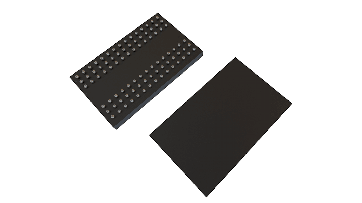
Winbond W949D2DBJX5I Mobile LPDDR SDRAM 512 MB Surface, 90-Pin 32 bit VFBGA
- RS-stocknr.:
- 188-2651
- Fabrikantnummer:
- W949D2DBJX5I
- Fabrikant:
- Winbond

Informatie over voorraden is momenteel niet toegankelijk
- RS-stocknr.:
- 188-2651
- Fabrikantnummer:
- W949D2DBJX5I
- Fabrikant:
- Winbond
Specificaties
Datasheets
Wetgeving en compliance
Productomschrijving
Zoek vergelijkbare producten door een of meer kenmerken te selecteren.
Alles selecteren | Attribuut | Waarde |
|---|---|---|
| Merk | Winbond | |
| Memory Size | 512MB | |
| Product Type | Mobile LPDDR SDRAM | |
| Organisation | 64M x 8 bit | |
| Data Bus Width | 32bit | |
| Address Bus Width | 15bit | |
| Number of Bits per Word | 8 | |
| Maximum Clock Frequency | 200MHz | |
| Maximum Random Access Time | 5ns | |
| Number of Words | 64M | |
| Mount Type | Surface | |
| Package Type | VFBGA | |
| Minimum Operating Temperature | -40°C | |
| Pin Count | 90 | |
| Maximum Operating Temperature | 85°C | |
| Length | 13.1mm | |
| Series | W949D2DB | |
| Standards/Approvals | LVCMOS Compatible | |
| Height | 0.65mm | |
| Width | 8.1mm | |
| Maximum Supply Voltage | 1.95V | |
| Automotive Standard | No | |
| Minimum Supply Voltage | 1.7V | |
| Alles selecteren | ||
|---|---|---|
Merk Winbond | ||
Memory Size 512MB | ||
Product Type Mobile LPDDR SDRAM | ||
Organisation 64M x 8 bit | ||
Data Bus Width 32bit | ||
Address Bus Width 15bit | ||
Number of Bits per Word 8 | ||
Maximum Clock Frequency 200MHz | ||
Maximum Random Access Time 5ns | ||
Number of Words 64M | ||
Mount Type Surface | ||
Package Type VFBGA | ||
Minimum Operating Temperature -40°C | ||
Pin Count 90 | ||
Maximum Operating Temperature 85°C | ||
Length 13.1mm | ||
Series W949D2DB | ||
Standards/Approvals LVCMOS Compatible | ||
Height 0.65mm | ||
Width 8.1mm | ||
Maximum Supply Voltage 1.95V | ||
Automotive Standard No | ||
Minimum Supply Voltage 1.7V | ||
VDD = 1.7∼1.95V
VDDQ = 1.7∼1.95V
Data width: x16 / x32
Clock rate: 200MHz (-5),166MHz (-6)
Standard Self Refresh Mode
Partial Array Self-Refresh(PASR)
Auto Temperature Compensated Self Refresh (ATCSR)
Power Down Mode
Deep Power Down Mode (DPD Mode)
Programmable output buffer driver strength
Four internal banks for concurrent operation
Data mask (DM) for write data
Clock Stop capability during idle periods
Auto Pre-charge option for each burst access
Double data rate for data output
Differential clock inputs (CK and CK)
Bidirectional, data strobe (DQS)
CAS Latency: 2 and 3
Burst Length: 2, 4, 8 and 16
Burst Type: Sequential or Interleave
8K refresh cycles/64 mS
Interface: LVCMOS compatible
Support package:
60 balls VFBGA (x16)
90 balls VFBGA (x32)
Operating Temperature Range
Extended: -25°C ≤ TCASE ≤ 85°C
Industrial: -40°C ≤ TCASE ≤ 85°C
This is a 512Mb Low Power DDR SDRAM organized as 2M words x 4 banks x 32bits.
Burst Type: Sequential or Interleave
Standard Self Refresh Mode
PASR, ATCSR, Power Down Mode、DPD
Programmable output buffer driver strength
Four internal banks for concurrent operation
Bidirectional, data strobe (DQS) is transmitted or received with data, to be used in capturing data at the receiver
Gerelateerde Links
- Winbond Mobile LPDDR SDRAM 512 MB Surface, 90-Pin 32 bit VFBGA
- Winbond Mobile LPDDR SDRAM 512 MB Surface, 60-Pin 16 bit VFBGA
- Winbond W949D6DBHX5I Mobile LPDDR SDRAM 512 MB Surface, 60-Pin 16 bit VFBGA
- Winbond SDRAM 512 MB Surface, 84-Pin 16 bit VFBGA
- Winbond W9751G6NB25I SDRAM 512 MB Surface, 84-Pin 16 bit VFBGA
- Micron MT46H32M16LFBF-5 IT:C SDRAM 512 MB Surface Mount, 60-Pin 16 bit VFBGA
- Winbond SDRAM 1 GB Surface, 60-Pin 16 bit VFBGA
- Winbond SDRAM 1 GB Surface, 96-Pin 16 bit VFBGA