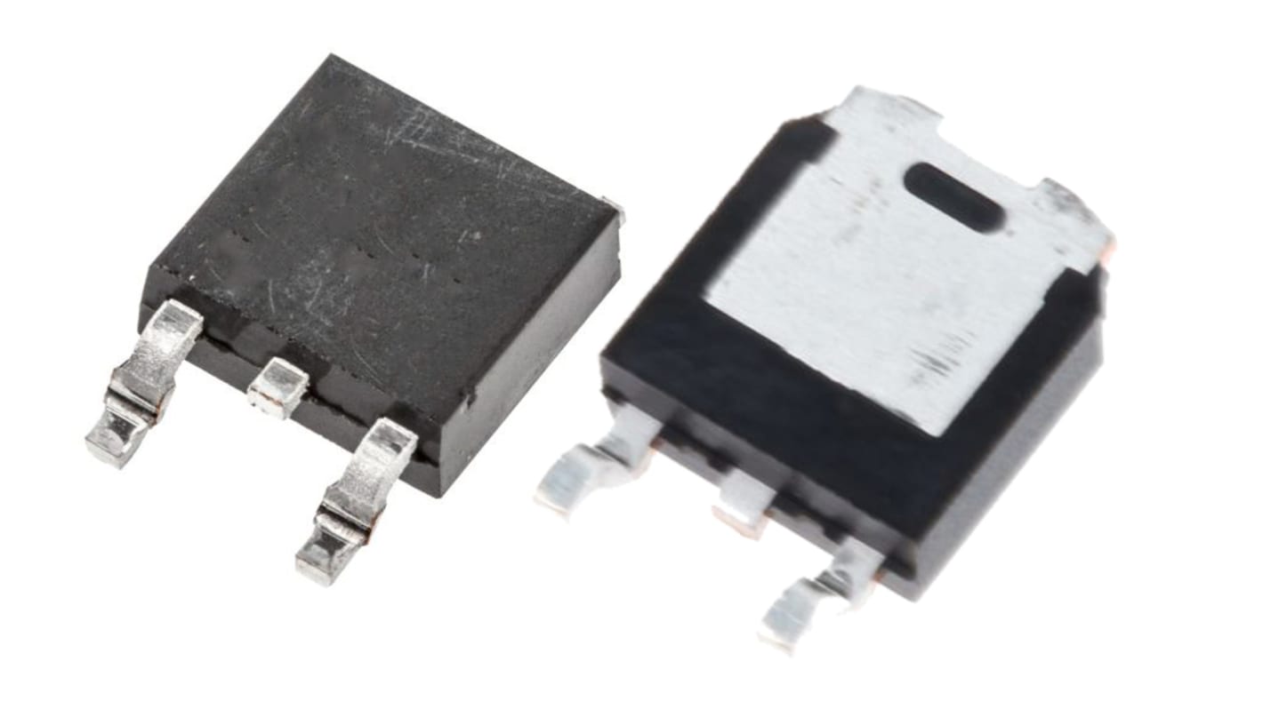
Vishay E Type N-Channel Power MOSFET, 4.4 A, 850 V Enhancement, 3-Pin TO-252 SiHD5N80AE-GE3
- RS-stocknr.:
- 228-2851
- Fabrikantnummer:
- SiHD5N80AE-GE3
- Fabrikant:
- Vishay

Subtotaal (1 rol van 3000 eenheden)*
€ 1.236,00
(excl. BTW)
€ 1.497,00
(incl. BTW)
GRATIS bezorging voor bestellingen van meer dan € 90,00
Tijdelijk niet op voorraad
- Verzending vanaf 23 december 2026
Heeft u meer nodig? Klik op 'Controleer leverdata' voor extra voorraad en levertijden.
Aantal stuks | Per stuk | Per rol* |
|---|---|---|
| 3000 + | € 0,412 | € 1.236,00 |
*prijsindicatie
- RS-stocknr.:
- 228-2851
- Fabrikantnummer:
- SiHD5N80AE-GE3
- Fabrikant:
- Vishay
Specificaties
Datasheets
Wetgeving en compliance
Productomschrijving
Zoek vergelijkbare producten door een of meer kenmerken te selecteren.
Alles selecteren | Attribuut | Waarde |
|---|---|---|
| Merk | Vishay | |
| Channel Type | Type N | |
| Product Type | Power MOSFET | |
| Maximum Continuous Drain Current Id | 4.4A | |
| Maximum Drain Source Voltage Vds | 850V | |
| Package Type | TO-252 | |
| Series | E | |
| Mount Type | Surface | |
| Pin Count | 3 | |
| Maximum Drain Source Resistance Rds | 1.35Ω | |
| Channel Mode | Enhancement | |
| Minimum Operating Temperature | -55°C | |
| Typical Gate Charge Qg @ Vgs | 11nC | |
| Maximum Power Dissipation Pd | 62.5W | |
| Maximum Gate Source Voltage Vgs | 30V | |
| Forward Voltage Vf | 1.2V | |
| Maximum Operating Temperature | 150°C | |
| Standards/Approvals | RoHS | |
| Automotive Standard | No | |
| Alles selecteren | ||
|---|---|---|
Merk Vishay | ||
Channel Type Type N | ||
Product Type Power MOSFET | ||
Maximum Continuous Drain Current Id 4.4A | ||
Maximum Drain Source Voltage Vds 850V | ||
Package Type TO-252 | ||
Series E | ||
Mount Type Surface | ||
Pin Count 3 | ||
Maximum Drain Source Resistance Rds 1.35Ω | ||
Channel Mode Enhancement | ||
Minimum Operating Temperature -55°C | ||
Typical Gate Charge Qg @ Vgs 11nC | ||
Maximum Power Dissipation Pd 62.5W | ||
Maximum Gate Source Voltage Vgs 30V | ||
Forward Voltage Vf 1.2V | ||
Maximum Operating Temperature 150°C | ||
Standards/Approvals RoHS | ||
Automotive Standard No | ||
Vishay Series E Power MOSFET, 850V Maximum Drain Source Voltage, 4.4A Maximum Continuous Drain Current - SiHD5N80AE-GE3
This power MOSFET is a high-voltage N-channel enhancement device designed for switching and power-conversion tasks in industrial electronics. It is supplied in a Compact surface-mount TO-252 package and is suited to applications that demand robust voltage handling and moderate continuous current capability in a small footprint.
Features and Benefits:
• 850V drain tolerance enables high-voltage system integration • 4.4A continuous drain current supports moderate load switching • 1.35Ω Rds(on) reduces conduction losses under load • 11nC typical gate charge allows efficient gate-drive design • 62.5W power dissipation manages thermal loading in Compact layouts • 150°C maximum junction temperature sustains high-temperature operation
Applications
• Suitable for SMPS and converters in industrial control systems • Ideal for flyback and boost topologies in power supplies • Used for line-side switching in LED drivers and lighting controls • Can be used for high-voltage pre-regulation stages in battery chargers
What gate-drive limits should be observed for safe operation?
The gate-source voltage must not exceed 30V to avoid gate-dielectric stress during switching transitions.
How does thermal margin affect PCB layout choices?
With a 62.5W dissipation rating and high junction capability, designers should provide adequate copper area or thermal vias to remove heat from the TO-252 land pattern.
Is this device suitable for automotive systems?
It is not specified for automotive-standard use and should not be selected where automotive qualification is mandatory.
What switching trade-offs arise from the gate-charge figure?
The 11nC gate charge balances switching speed and drive energy, requiring gate drivers sized for the desired rise/fall times and switching frequency.
Gerelateerde Links
- Vishay E Type N-Channel Power MOSFET 850 V Enhancement, 3-Pin TO-252 SiHD5N80AE-GE3
- Vishay E Type N-Channel MOSFET 850 V Enhancement, 3-Pin TO-252
- Vishay E Type N-Channel MOSFET 850 V Enhancement, 3-Pin TO-252 SIHD6N80AE-GE3
- Vishay E Type N-Channel Power MOSFET 850 V Enhancement, 3-Pin TO-252
- Vishay E Type N-Channel Power MOSFET 850 V Enhancement, 3-Pin TO-252 SIHD11N80AE-T1-GE3
- Vishay E Type N-Channel Power MOSFET 800 V Enhancement, 3-Pin IPAK
- Vishay E Type N-Channel Power MOSFET 800 V Enhancement, 3-Pin IPAK SIHU5N80AE-GE3
- Vishay E Type N-Channel MOSFET 850 V Enhancement, 3-Pin TO-220