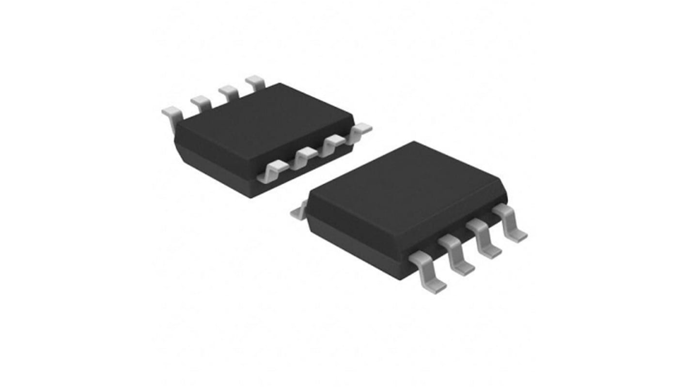
Vishay Si4948BEY Type P-Channel MOSFET, -2.4 A, -60 V, 8-Pin SOIC
- RS-stocknr.:
- 256-7362
- Fabrikantnummer:
- SI4948BEY-T1-E3
- Fabrikant:
- Vishay

Subtotaal (1 rol van 2500 eenheden)*
€ 1.242,50
(excl. BTW)
€ 1.502,50
(incl. BTW)
GRATIS bezorging voor bestellingen van meer dan € 90,00
Tijdelijk niet op voorraad
- Verzending vanaf 16 september 2026
Heeft u meer nodig? Klik op 'Controleer leverdata' voor extra voorraad en levertijden.
Aantal stuks | Per stuk | Per rol* |
|---|---|---|
| 2500 + | € 0,497 | € 1.242,50 |
*prijsindicatie
- RS-stocknr.:
- 256-7362
- Fabrikantnummer:
- SI4948BEY-T1-E3
- Fabrikant:
- Vishay
Specificaties
Datasheets
Wetgeving en compliance
Productomschrijving
Zoek vergelijkbare producten door een of meer kenmerken te selecteren.
Alles selecteren | Attribuut | Waarde |
|---|---|---|
| Merk | Vishay | |
| Channel Type | Type P | |
| Product Type | MOSFET | |
| Maximum Continuous Drain Current Id | -2.4A | |
| Maximum Drain Source Voltage Vds | -60V | |
| Series | Si4948BEY | |
| Package Type | SOIC | |
| Mount Type | Surface | |
| Pin Count | 8 | |
| Maximum Drain Source Resistance Rds | 0.15Ω | |
| Maximum Power Dissipation Pd | 1.4W | |
| Forward Voltage Vf | -1.2V | |
| Maximum Gate Source Voltage Vgs | 20V | |
| Typical Gate Charge Qg @ Vgs | 14.5nC | |
| Minimum Operating Temperature | -55°C | |
| Maximum Operating Temperature | 175°C | |
| Standards/Approvals | RoHS 2002/95/EC, IEC 61249-2-21 | |
| Height | 1.75mm | |
| Automotive Standard | No | |
| Alles selecteren | ||
|---|---|---|
Merk Vishay | ||
Channel Type Type P | ||
Product Type MOSFET | ||
Maximum Continuous Drain Current Id -2.4A | ||
Maximum Drain Source Voltage Vds -60V | ||
Series Si4948BEY | ||
Package Type SOIC | ||
Mount Type Surface | ||
Pin Count 8 | ||
Maximum Drain Source Resistance Rds 0.15Ω | ||
Maximum Power Dissipation Pd 1.4W | ||
Forward Voltage Vf -1.2V | ||
Maximum Gate Source Voltage Vgs 20V | ||
Typical Gate Charge Qg @ Vgs 14.5nC | ||
Minimum Operating Temperature -55°C | ||
Maximum Operating Temperature 175°C | ||
Standards/Approvals RoHS 2002/95/EC, IEC 61249-2-21 | ||
Height 1.75mm | ||
Automotive Standard No | ||
Vishay Si4948BEY Series MOSFET, -60V Drain Source Voltage, -2.4A Continuous Drain Current - SI4948BEY-T1-E3
This MOSFET is a P‑channel surface‑mount transistor designed for switching and power‑control tasks in electronic systems. It operates within a wide temperature envelope and is intended for use on Compact boards where an SOIC package and moderate power handling are required. The device suits engineers needing a P‑channel option with specific gate charge and thermal limits for circuit‑level design.
Features and Benefits:
• P‑channel device supporting negative drain‑source voltage for high‑side switching • Rated drain‑source voltage of -60V enabling elevated voltage applications • Maximum continuous drain current -2.4A allowing moderate load handling • Low on‑resistance 0.15Ω reducing conduction losses • Typical gate charge 14.5nC facilitating predictable switching behaviour • Power dissipation 1.4W managing thermal budget in confined layouts
Applications
• Suitable for high‑side switches in motor control modules • Ideal for load disconnects in power management circuits • Used for reverse polarity protection in supply rails • Can be used for battery management and charging control • Suitable for SMD assemblies requiring Compact P‑channel transistors
What gate voltage limits should be observed during design?
The gate‑source voltage must not exceed ±20V to prevent gate oxide stress and ensure reliable operation.
How does the device behave at elevated temperatures?
It is specified to operate up to 175°C maximum, so designers should account for derating of current and power with temperature rise.
What package and pin count are available for PCB layout considerations?
The component is supplied in an SOIC‑8 package with eight pins, suitable for standard SMD footprint designs.
Which standards relate to material and process acceptability?
The component complies with RoHS 2002/95/EC and follows IEC 61249‑2‑21 material specifications.
What forward voltage or body diode characteristic is indicated?
A forward voltage of -1.2V is specified for the intrinsic diode conduction behaviour.
Gerelateerde Links
- Vishay Si4948BEY Type N-Channel MOSFET 60 V, 8-Pin SOIC SI4948BEY-T1-E3
- Vishay Isolated TrenchFET 2 Type P-Channel MOSFET 60 V Enhancement, 8-Pin SOIC SI4948BEY-T1-GE3
- Vishay Isolated TrenchFET 2 Type P-Channel MOSFET 60 V Enhancement, 8-Pin SOIC
- Vishay Si4850EY Type N-Channel MOSFET 60 V Enhancement, 8-Pin SOIC
- Vishay Type N-Channel MOSFET 60 V, 8-Pin PowerPAK 1212-8
- Vishay Si4850EY Type N-Channel MOSFET 60 V Enhancement, 8-Pin SOIC SI4850EY-T1-GE3
- Vishay Isolated Type N-Channel MOSFET 60 V Enhancement, 8-Pin SOIC SI9945BDY-T1-GE3
- Vishay SQ Rugged Type N-Channel MOSFET 60 V Enhancement, 8-Pin SOIC