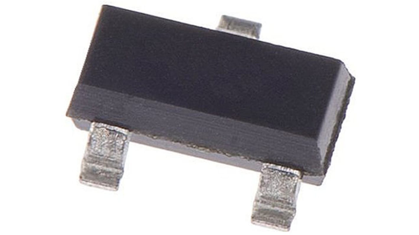
Vishay Si2325DS Type P-Channel MOSFET, -530 mA, -150 V Enhancement, 3-Pin SOT-23 SI2325DS-T1-E3
- RS-stocknr.:
- 710-3263
- Fabrikantnummer:
- SI2325DS-T1-E3
- Fabrikant:
- Vishay

Subtotaal (1 verpakking van 5 eenheden)*
€ 5,14
(excl. BTW)
€ 6,22
(incl. BTW)
GRATIS bezorging voor bestellingen van meer dan € 90,00
Op voorraad
- 5 stuk(s) klaar voor verzending vanaf een andere locatie
- Plus verzending 2.030 stuk(s) vanaf 21 juli 2026
Heeft u meer nodig? Klik op 'Controleer leverdata' voor extra voorraad en levertijden.
Aantal stuks | Per stuk | Per verpakking* |
|---|---|---|
| 5 + | € 1,028 | € 5,14 |
*prijsindicatie
- RS-stocknr.:
- 710-3263
- Fabrikantnummer:
- SI2325DS-T1-E3
- Fabrikant:
- Vishay
Specificaties
Datasheets
Wetgeving en compliance
Productomschrijving
Zoek vergelijkbare producten door een of meer kenmerken te selecteren.
Alles selecteren | Attribuut | Waarde |
|---|---|---|
| Merk | Vishay | |
| Product Type | MOSFET | |
| Channel Type | Type P | |
| Maximum Continuous Drain Current Id | -530mA | |
| Maximum Drain Source Voltage Vds | -150V | |
| Series | Si2325DS | |
| Package Type | SOT-23 | |
| Mount Type | Surface | |
| Pin Count | 3 | |
| Maximum Drain Source Resistance Rds | 1.2Ω | |
| Channel Mode | Enhancement | |
| Maximum Gate Source Voltage Vgs | 20V | |
| Typical Gate Charge Qg @ Vgs | 7.7nC | |
| Maximum Power Dissipation Pd | 750mW | |
| Minimum Operating Temperature | -55°C | |
| Forward Voltage Vf | -1.2V | |
| Maximum Operating Temperature | 150°C | |
| Height | 1.02mm | |
| Length | 3.04mm | |
| Width | 1.4mm | |
| Standards/Approvals | RoHS | |
| Automotive Standard | No | |
| Alles selecteren | ||
|---|---|---|
Merk Vishay | ||
Product Type MOSFET | ||
Channel Type Type P | ||
Maximum Continuous Drain Current Id -530mA | ||
Maximum Drain Source Voltage Vds -150V | ||
Series Si2325DS | ||
Package Type SOT-23 | ||
Mount Type Surface | ||
Pin Count 3 | ||
Maximum Drain Source Resistance Rds 1.2Ω | ||
Channel Mode Enhancement | ||
Maximum Gate Source Voltage Vgs 20V | ||
Typical Gate Charge Qg @ Vgs 7.7nC | ||
Maximum Power Dissipation Pd 750mW | ||
Minimum Operating Temperature -55°C | ||
Forward Voltage Vf -1.2V | ||
Maximum Operating Temperature 150°C | ||
Height 1.02mm | ||
Length 3.04mm | ||
Width 1.4mm | ||
Standards/Approvals RoHS | ||
Automotive Standard No | ||
- Land van herkomst:
- CN
Vishay Si2325DS Series MOSFET, -150V Maximum Drain Source Voltage, 1.2Ω Maximum Drain Source Resistance - SI2325DS-T1-E3
This p-channel MOSFET is a surface-mount semiconductor device designed for high-voltage switching and control in Compact assemblies. It functions as an enhancement-mode transistor suitable for use where reverse-polarity or high-side switching is required, and is optimised for low-power dissipation in small form-factor SOT-23 packages. The device operates across a wide temperature range, making it appropriate for varied industrial electronic contexts.
Features and Benefits:
• Maximum drain-source voltage supports 150V applications • Drain-source resistance of 1.2Ω reduces conduction losses • Continuous drain current of -530mA permits modest load driving • Typical gate charge of 7.7nC enables Faster gate transitions • Power dissipation rating of 750mW limits thermal build-up • Gate-source voltage tolerance of 20V allows robust drive margins
Applications
• Suitable for high-voltage load switching in automation systems • Ideal for high-side switching in control and power modules • Used for reverse-polarity protection in electronic designs • Can be used for level-shifted gate-drive circuits • Suitable for Compact power-management boards in instrumentation
What are the thermal limits for reliable operation?
The device is specified to operate between -55°C and 150°C, allowing use across typical industrial temperature ranges.
How does the package influence board layout?
The SOT-23 surface-mount package with three pins and Compact footprint supports dense assembly and straightforward thermal via placement for heat management.
What electrical constraint should designers observe for gate driving?
Designers must restrict gate-source voltage within ±20V to avoid gate dielectric stress and ensure long-term reliability.
How should power dissipation considerations affect cooling strategy?
With a 750mW dissipation rating, designers should provide adequate copper area or heatsinking on the PCB to maintain junction temperatures under load.
Gerelateerde Links
- Vishay Si2325DS Type P-Channel MOSFET -150 V Enhancement, 3-Pin SOT-23
- Vishay TP0610K Type P-Channel MOSFET 60 V Enhancement, 3-Pin SOT-23 TP0610K-T1-E3
- Vishay TrenchFET Type P-Channel MOSFET 20 V Enhancement, 3-Pin SOT-23 SI2301CDS-T1-E3
- Vishay P-Channel MOSFET Transistor 20 V, 3-Pin SOT-23 SI2301BDS-T1-E3
- Vishay TP0610K Type P-Channel MOSFET 60 V Enhancement, 3-Pin SOT-23
- Vishay TrenchFET Type P-Channel MOSFET 20 V Enhancement, 3-Pin SOT-23
- Vishay Si2328DS Type N-Channel MOSFET 100 V Enhancement, 3-Pin SOT-23 SI2328DS-T1-E3
- Vishay TrenchFET Type N-Channel Power MOSFET 60 V Enhancement, 3-Pin SOT-23 SI2308BDS-T1-E3